Sep 7, 2026Industry
Precision Machining for Optical Mounts & Semiconductor Components: What Buyers Need to Know
Optical mounts and semiconductor components need more than tight tolerances: outgassing control, stray light management, thermal stability and cleanroom-level cleanliness. What to demand from your mac
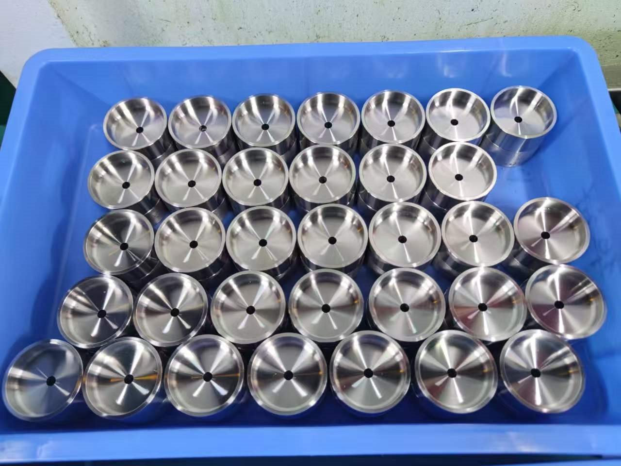
Introduction
Precision machining for optical instruments and semiconductor equipment is a different discipline from everyday CNC work. Surfaces that are acceptable in a robot arm are unacceptable in a laser housing. A shadow on a lens mount ruins the alignment. A particle inside a vacuum chamber ruins the process.
If you are buying machined components for these industries, here is what actually matters — from material selection to cleanliness to inspection — and what to ask your supplier.
Why optical and semiconductor parts are a different class
Three enemies dominate:
Outgassing. Components in ultra-high-vacuum chambers must not release trapped air, cutting fluid or residue — micro-pores in the material or leftover contaminants evaporate into the vacuum and wreck the process.
Stray light. Inside laser housings and lens mounts, reflections from imperfectly treated surfaces scatter light off the optical path.
Thermal drift. Residual stress and temperature changes shift geometry by microns — enough to misalign an optical system or alter a semiconductor process.
A machining supplier that only quotes tolerances is answering the wrong question. These parts need a process, not just a number.
Outgassing control: cleanliness starts in the material
The fight against outgassing starts before machining:
Dense material selection. Aluminum and stainless steel that have passed ultrasonic flaw detection, so microscopic material pores are eliminated from the source
Ultrasonic cleaning after machining. A professional multi-tank ultrasonic cleaning line uses combined frequencies and eco-friendly solvents to strip cutting fluid and residue from the part surface
Cleanroom double-bagging immediately after cleaning. Parts move directly to a cleanroom where they are wrapped with cleanroom-grade, lint-free materials under controlled conditions
Ask your supplier for the cleaning process, not a "we clean them" statement.
Stray light control: matte black anodizing done right
Optical parts that surround the light path need surfaces that absorb instead of reflect. The standard solution is matte black anodizing:
Sandblasting creates a controlled micro-roughness before anodizing
Black anodizing produces a matte surface with very low reflectivity, absorbing stray light to keep the optical path clean
Look for suppliers who describe the full sequence (blasting plus anodizing) and can show finished parts — not just an anodize color code on the quote.
Thermal stability: process and geometry
Thermal stability comes from two directions:
Environmental control. Temperature-controlled machining keeps the shop environment and the part within the range where microns stay put during critical tolerance cuts
Material choice with purpose. Copper for heat-managed components like base plates, high-purity aluminum for vacuum and structural parts, brass where conductivity and clean threading matter
Combined with the standard-tolerance reality — ±0.01mm to ±0.05mm as the everyday band and up to ±0.005mm at high precision, geometry permitting — these parts are won by process discipline, not by a single impressive number on a quote.
The parts that show up most often
Typical machined components in this world (and close relatives):
Lens mounts, optical benches and alignment fixtures
Laser housings and heat-managed aluminum housings
Wafer handling and transfer components
Vacuum chamber components in high-purity aluminum or stainless
Copper base plates and custom heat sinks for power electronics
Precision connector contacts, gold-plated for signal integrity
What your inspection paperwork should show
For optical and semiconductor work, inspection documents are non-negotiable:
First Article Inspection and CMM-based results on critical features
Material certificates (CoC) matching your alloy callout — high-purity aluminum vs standard grades is a real difference
100% inspection records before shipment
Cleanliness evidence where the application needs it (cleaning process + packaging method)
If the supplier cannot describe each of these before quoting, they are not ready for this class of parts.
The practical checklist when sourcing
Specify material purity and grade explicitly (plus any cleanliness requirement)
State the surface spec with the process: sandblasting + black anodizing for stray light; passivation for stainless in clean environments
Call out tolerances only on functional features — optical bores, mounting datums, sealing faces
Ask for the cleaning and packaging procedure in writing (cleanroom double-bagging for vacuum-use parts)
Demand the inspection plan at quote stage: FAI, CMM, CoC, 100% inspection
Confirm the DFM review happens before cutting — small geometry changes save real cost
Your next step
Send your optical or semiconductor drawing to a shop that documents its process — for example, Idar Tech in Dongguan, China (ISO 9001:2015): tolerance control to ±0.005mm, ultrasonic cleaning and cleanroom packaging lines, matte black anodizing and plating supply chain, CMM-verified inspection — with a free DFM review and itemized quote within 24 hours.