Jun 26, 2026Industry
Advanced Machining Solutions for Semiconductor & Optical Equipment
In the fields of semiconductor manufacturing and high-end optical instruments, we understand a harsh reality: even a micron-level deviation or a microscopic trace of residual oil is enough to ruin m
In the fields of semiconductor manufacturing and high-end optical instruments, we understand a harsh reality: even a micron-level deviation or a microscopic trace of residual oil is enough to ruin million-dollar wafers or cause expensive optical systems to fail completely.
As a Chinese precision machining factory with deep industry expertise, we have long supplied global clients with core components such as wafer transfer arms, vacuum chambers, laser housings, and high-precision lens mounts. We are not just "machinists"; we are your "technical partners" who truly understand the physical operating environments of your equipment.
Addressing the top three pain points that trouble semiconductor and optical equipment clients the most, we provide transparent, professional answers and solutions below.
Pain Point 1: The "Outgassing" Disaster in High-Vacuum Environments
Client's Concern: Semiconductor equipment (like PVD/CVD chambers) operates under ultra-high vacuum. If there are micro-pores inside the material, or if cutting fluids and oils are left behind due to poor cleaning, these substances will "outgas" in the vacuum, directly contaminating and ruining entire batches of wafers.
Our Solution: Ultrasonic Cleaning & Strict Cleanroom Packaging
To completely eliminate outgassing, we have established a rigorous "Purity Control" process:
- Dense Material Selection: We only use premium aluminum alloys and stainless steel that have passed ultrasonic flaw detection, eliminating microscopic pores from the source.
- Medical-Grade Ultrasonic Cleaning Line: After machining, parts enter our professional multi-tank ultrasonic cleaning line. Using different ultrasonic frequencies combined with eco-friendly solvents, we thoroughly strip away micro-chips and oil molecules hidden in blind holes and deep threads.
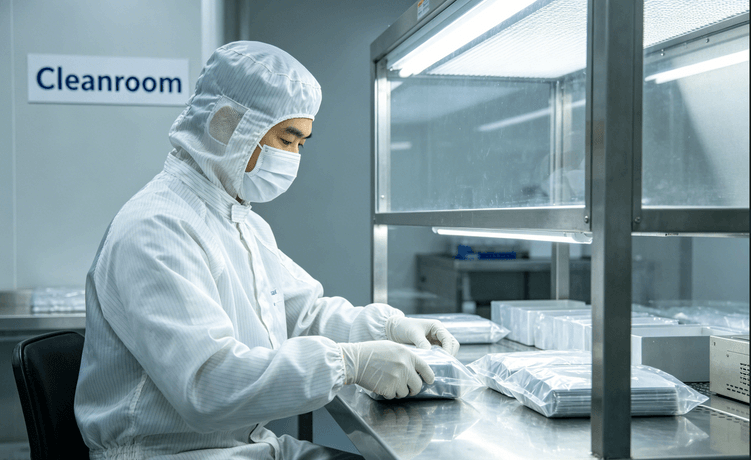
- Cleanroom Double-Bagging Protocol: Cleaned parts are immediately transferred to our ISO-certified Cleanroom. Workers in anti-static cleanroom suits use cleanroom-grade, lint-free materials to wrap the parts, followed by a strict double-bagging and heat-sealing process. This multi-layer protection ensures that no particulate matter or external contaminants reach the parts during transit, keeping them pristine and ready for your critical assembly lines.
Pain Point 2: "Stray Light" in Optical Systems & Surface Treatment Challenges
Client's Concern: Inside laser housings or high-precision lens mounts, improper surface treatment can cause reflections and stray light, severely disrupting the optical path. Meanwhile, parts also require extremely high wear and corrosion resistance.
Our Solution: Comprehensive Surface Treatment Expertise
We have a deeply integrated and strictly certified surface treatment supply chain, perfectly meeting the demanding requirements of the optical and semiconductor industries:
* Matte Black Anodizing: Custom-designed for optical parts. Through specific sandblasting and anodizing processes, we create a matte black surface with extremely low reflectivity, perfectly absorbing stray light to ensure a pure optical path.
* Hard Anodizing: For moving parts like wafer transfer arms, we provide high-thickness, high-hardness hard anodizing. This significantly improves wear resistance and electrical insulation without generating micro-dust shedding.
* Electroless Nickel Plating: For vacuum chamber components requiring extreme corrosion resistance and strict dimensional control, electroless nickel plating provides a highly uniform coating. It maintains consistent thickness even in complex internal cavities and blind holes, preserving the part's original precision.
Pain Point 3: Thermal Expansion Deformation & The "Ultra-High Precision" Challenge
Client's Concern: Optical instruments require extreme precision for optical alignment. Residual stress from machining or slight temperature changes in the operating environment can cause micron-level deformation. Just how tight can you hold your tolerances?
Our Solution: Temperature-Controlled Machining & ±0.002mm Extreme Tolerances
"High precision" is not just a slogan in our factory; it is a quantifiable metric guaranteed by our equipment, environment, and processes:
1. Pushing the Limits of Tolerance: Relying on imported high-end 5-axis CNC machining centers and experienced programming engineers, we consistently control the tolerances of critical dimensions between ±0.002mm and ±0.005mm. Whether it's concentricity, flatness, or perpendicularity, we meet the most stringent drawing requirements.
2. Stress Relief & Temperature Control: For thin-walled parts prone to deformation (like large lens mounts), we add a "stress relief annealing" process after rough machining. Furthermore, our precision machining workshop and CMM inspection room are under strict 24/7 constant temperature and humidity control, completely eliminating the interference of thermal expansion and contraction.
3. Full Dimensional Inspection Reports: Every precision part delivered comes with a First Article Inspection Report (FAIR) generated by a high-precision Coordinate Measuring Machine (CMM), making the precision data completely transparent.
Conclusion: Your Most Reliable Precision Manufacturing Backbone
In the semiconductor and optical equipment industries, there is no "good enough"—there is only "absolute precision" and "absolute purity."
As a professional Chinese precision machining factory, we provide not only metal cutting services that meet ±0.002mm tolerances but also a one-stop solution ranging from specialized surface treatments (Matte Black/Hard Anodizing/Electroless Nickel) to ultrasonic cleaning and strict cleanroom double-bagging.
If you are looking for a reliable supplier who truly understands the dangers of "Outgassing" and knows how to control optical stray light, please send us your drawings. Our engineering team will provide a professional Design for Manufacturability (DFM) analysis and quote within 24 hours.
Contact us today, and let your next-generation semiconductor and optical equipment win at the starting line.